The STM32F101x4 and STM32F101x6 Low-density access line family incorporates the high-performance ARM Cortex™-M3 32-bit RISC core operating at a 36 MHz frequency, high-speed embedded memories (Flash memory of 16 to 32 Kbytes and SRAM of 4 to 6 Kbytes), and an extensive range of enhanced peripherals and I/Os connected to two APB buses. All devices offer standard communication interfaces (one I2C, one SPI, and two USARTs), one 12-bit ADC and up to two general-purpose 16-bit timers.
The STM32F101xx Low-density access line family operates in the –40 to +85 ℃ temperature range, from a 2.0 to 3.6 V power supply. A comprehensive set of power-saving mode allows the design of low-power applications.
The STM32F101xx Low-density access line family includes devices in three different packages ranging from 36 pins to 64 pins. Depending on the device chosen, different sets of peripherals are included, the description below gives an overview of the complete range of peripherals proposed in this family.
These features make the STM32F101xx Low-density access line microcontroller family suitable for a wide range of applications such as application control and user interface,medical and handheld equipment, PC peripherals, gaming and GPS platforms, industrial applications, PLCs, inverters, printers, scanners, alarm systems, Video intercoms, and HVACs.
STM32F101x4 和STM32F101x6主要特性:
■ Core: ARM 32-bit Cortex™-M3 CPU
– 36 MHz maximum frequency,1.25 DMIPS/MHz (Dhrystone 2.1) performance at 0 wait state memory access
– Single-cycle multiplication and hardware division
■ Memories
– 16 to 32 Kbytes of Flash memory
– 4 to 6 Kbytes of SRAM
■ Clock, reset and supply management
– 2.0 to 3.6 V application supply and I/Os
– POR, PDR and programmable voltage detector (PVD)
– 4-to-16 MHz crystal oscillator
– Internal 8 MHz factory-trimmed RC
Internal 40 kHz RC
PLL for CPU clock
– 32 kHz oscillator for RTC with calibration
■ Low power
– Sleep, Stop and Standby modes
– VBAT supply for RTC and backup registers
■ Debug mode
– Serial wire debug (SWD) and JTAG interfaces
■ DMA
– 7-channel DMA controller
– Peripherals supported: timers, ADC, SPIs, I2Cs and USARTs
■ 1 × 12-bit, 1 μs A/D converter (up to 16 channels)
– Conversion range: 0 to 3.6 V
– Temperature sensor
■ Up to 51 fast I/O ports
– 26/37/51 I/Os, all mappable on 16 external interrupt vectors and almost all 5 V-tolerant
■ Up to 5 timers
– Up to two16-bit timers, each with up to 4 IC/OC/PWM or pulse counter
2 watchdog timers (Independent and Window)
– SysTick timer: 24-bit downcounter
■ Up to 4 communication interfaces
– 1 x I2C interface (SMBus/PMBus)
– Up to 2 USARTs (ISO 7816 interface, LIN, IrDA capability, modem control)
– 1 × SPI (18 Mbit/s)
■ CRC calculation unit, 96-bit unique ID
■ ECOPACK® packages

图1.STM32F101x4 和STM32F101x6方框图
The solar-LED streetlight controller consists of one 80 W battery charger and one 25 W LED driver. During the daytime, when there is sufficient sunlight, the charger converts the electricity from the solar panel and charges the battery. At nighttime, the battery powers on the LED lamp as streetlight.
If it is rainy or cloudy for several continuous days, the battery will gradually run out of power. The controller then resorts to the AC mains supply to power on the LED until the battery has had time to fully charge again.
太阳能LED街灯控制器主要特性:
■ Maximization of electricity conversion efficiency from solar panel by way of maximum power point tracker (MPPT)
■ Automatic day/night/weather detection
■ Automatic battery/mains switch over
■ Constant current control for LED lamp
■ Battery charge control
■ Optional LED lighting duration mode
■ Easy system monitoring via debug LED indicators
■ Full protection function for OTP, OCP and UVP

图2.太阳能LED街灯控制器外形图

图3.太阳能LED街灯控制系统方框图

图4.太阳能LED街灯控制器电路图
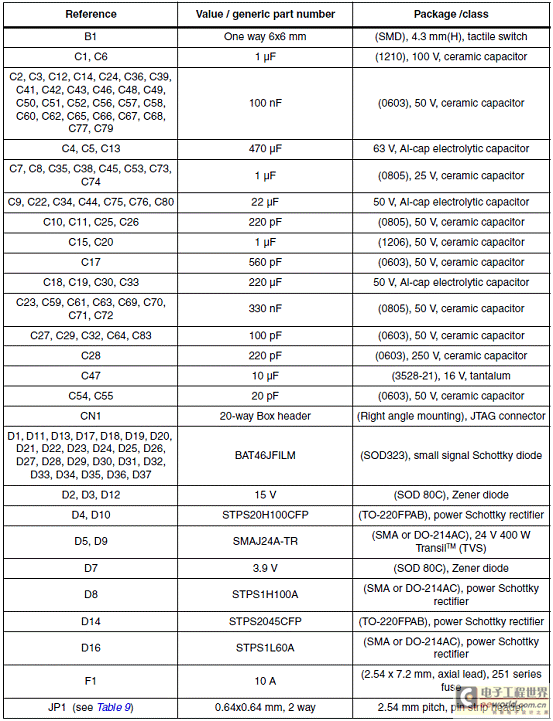
太阳能LED街灯控制器材料清单(BOM):


上一篇:有源纹波补偿BUCK型LED驱动电路设计
下一篇:适用于高能效多灯串系统的完整街道照明平台的数字LED驱动器解决方案
推荐阅读最新更新时间:2023-10-18 15:36


Vishay线上图书馆
- 选型-汽车级表面贴装和通孔超快整流器
- 你知道吗?DC-LINK电容在高湿条件下具有高度稳定性
- microBUCK和microBRICK直流/直流稳压器解决方案
- SOP-4小型封装光伏MOSFET驱动器VOMDA1271
- 使用薄膜、大功率、背接触式电阻的优势
- SQJQ140E车规级N沟道40V MOSFET


 门老师教你学电子——电子电路识图 (门宏)
 Verilog HDL数字集成电路设计原理与应用


 京公网安备 11010802033920号