A typical +12V, 6A, hot-swap controller circuit (Figure 1) contains (like many others) slow and fast comparators with trip thresholds of 50mV and 200mV. The 6mΩ Sense resistor (RS) allows a nominal slow-comparator trip at 8.3A for overload conditions, and a fast-comparator trip at 33.3A for short circuits.
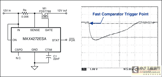
Figure 1. Typical hot-swap controller circuit exhibits a 30ms short-circuit current pulse of 400A peak.
The initial short-circuit current spike is limited only by circuit resistances¹ during a period that includes the fast-comparator delay and the 30µs it takes to complete interruption of the short circuit by discharging M1's gate capacitance. The waveform recorded during a short circuit indicates a peak current of 400A (due to 2.4Vpk across Rs), decreasing to 100A in 28µs.
The short-circuit current duration can be limited to ≤ 0.5ms by adding a Darlington pnp transistor (Q1) to speed the gate discharge (Figure 2). D1 allows the gate to charge normally at turn-on, but at turn-off the controller's 3mA gate-discharge current is directed to the base of Q1. Q1 then acts quickly to discharge the gate, in ≤ 100ns. Thus, the high-current portion of the short circuit is limited to slightly more than the fast-comparator's delay time of 350ns.
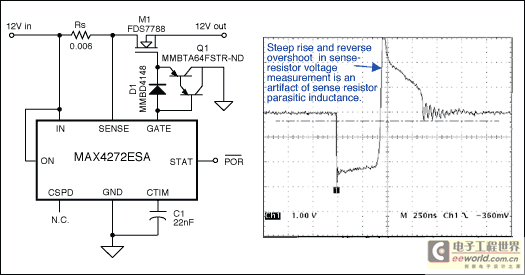
Figure 2. The addition of Q1 increases the gate-pulldown current, limiting the short-circuit current duration to less than 0.5ms.
The apparent reverse overshoot current and the steep rise seen in the waveforms of Figures 2 and 3 is created by parasitic series inductance in the sense resistor chip, and the leading-edge oscillation seen in Figure 3 is an artifact introduced by the oscilloscope ground lead.
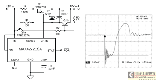
Figure 3. Hot-swap controller with fast limiting of short-circuit current peaks, and short-circuit waveform.
The circuit of Figure 3 can limit short-circuit current to ≈100A for < 200ns. The pnp transistor Q1a, which is triggered when the voltage across RS reaches ≈600mV, drives the npn transistor Q1b to quickly discharge M1's gate capacitance. Quick triggering of the pnp transistor is aided by the steep voltage waveform, which in turn is a result of parasitic inductance in the sense-resistor.
C2 is connected between the gate and source of M1 to reduce the positive transient step voltage applied to the gate during a short circuit. Zener diode D1 reduces ID(ON) by limiting VGS to something less than the 7V available from the MAX4272. Although D1 is rated 5.1V when biased at 5mA, it limits VGS to ≈3.4V in this circuit because only 100mA of gate-charging current (zener bias current) is available from the IC. The limited VGS lowers ID(ON)—at some expense to RD(ON)—and allows a quicker turn off of M1. D1 and C2 can also be employed to some advantage in Figure 1 and Figure 2, to reduce ID(ON) during short circuits.
Either of the two circuits above can protect a backplane power source by minimizing the energy dissipated when a hot-swap-controlled circuit is shorted. The simpler circuit (Figure 2) dramatically shortens the short-circuit-current interval to somewhat less than 500ns, and the slightly more complex circuit (Figure 3) reduces the peak short-circuit current to 100A, as well as truncating the pulse width to less than 200ns. Either technique can be applied to most hot-swap controller circuits. Individual results vary² according to the impedance of the power source, the impedance of the short circuit, and (especially) the quality and attack time of the short circuit itself.
¹Source resistance, short-circuit quality, value of RS, MOSFET's RDS(ON), and MOSFET's ID(ON).
²Note that it is inordinately difficult to achieve a repeatable low-resistance short circuit by manual manipulation of a shorting bar. Careful layout and low-ESR capacitors are required to create a power source with very low ESR.
This design idea appeared in the May 27, 2004 issue of EDN.
编辑:神话 引用地址:尽量减少短路电流脉冲的热插拔控制器-Minimize Sho

Figure 1. Typical hot-swap controller circuit exhibits a 30ms short-circuit current pulse of 400A peak.
The initial short-circuit current spike is limited only by circuit resistances¹ during a period that includes the fast-comparator delay and the 30µs it takes to complete interruption of the short circuit by discharging M1's gate capacitance. The waveform recorded during a short circuit indicates a peak current of 400A (due to 2.4Vpk across Rs), decreasing to 100A in 28µs.
The short-circuit current duration can be limited to ≤ 0.5ms by adding a Darlington pnp transistor (Q1) to speed the gate discharge (Figure 2). D1 allows the gate to charge normally at turn-on, but at turn-off the controller's 3mA gate-discharge current is directed to the base of Q1. Q1 then acts quickly to discharge the gate, in ≤ 100ns. Thus, the high-current portion of the short circuit is limited to slightly more than the fast-comparator's delay time of 350ns.

Figure 2. The addition of Q1 increases the gate-pulldown current, limiting the short-circuit current duration to less than 0.5ms.
The apparent reverse overshoot current and the steep rise seen in the waveforms of Figures 2 and 3 is created by parasitic series inductance in the sense resistor chip, and the leading-edge oscillation seen in Figure 3 is an artifact introduced by the oscilloscope ground lead.

Figure 3. Hot-swap controller with fast limiting of short-circuit current peaks, and short-circuit waveform.
The circuit of Figure 3 can limit short-circuit current to ≈100A for < 200ns. The pnp transistor Q1a, which is triggered when the voltage across RS reaches ≈600mV, drives the npn transistor Q1b to quickly discharge M1's gate capacitance. Quick triggering of the pnp transistor is aided by the steep voltage waveform, which in turn is a result of parasitic inductance in the sense-resistor.
C2 is connected between the gate and source of M1 to reduce the positive transient step voltage applied to the gate during a short circuit. Zener diode D1 reduces ID(ON) by limiting VGS to something less than the 7V available from the MAX4272. Although D1 is rated 5.1V when biased at 5mA, it limits VGS to ≈3.4V in this circuit because only 100mA of gate-charging current (zener bias current) is available from the IC. The limited VGS lowers ID(ON)—at some expense to RD(ON)—and allows a quicker turn off of M1. D1 and C2 can also be employed to some advantage in Figure 1 and Figure 2, to reduce ID(ON) during short circuits.
Either of the two circuits above can protect a backplane power source by minimizing the energy dissipated when a hot-swap-controlled circuit is shorted. The simpler circuit (Figure 2) dramatically shortens the short-circuit-current interval to somewhat less than 500ns, and the slightly more complex circuit (Figure 3) reduces the peak short-circuit current to 100A, as well as truncating the pulse width to less than 200ns. Either technique can be applied to most hot-swap controller circuits. Individual results vary² according to the impedance of the power source, the impedance of the short circuit, and (especially) the quality and attack time of the short circuit itself.
¹Source resistance, short-circuit quality, value of RS, MOSFET's RDS(ON), and MOSFET's ID(ON).
²Note that it is inordinately difficult to achieve a repeatable low-resistance short circuit by manual manipulation of a shorting bar. Careful layout and low-ESR capacitors are required to create a power source with very low ESR.
This design idea appeared in the May 27, 2004 issue of EDN.
上一篇:CCFL推挽式缓冲电路
下一篇:DS3906电阻计算器
- 热门资源推荐
- 热门放大器推荐
小广播
热门活动
换一批
更多
最新模拟电子文章
更多精选电路图
更多热门文章
更多每日新闻
- Allegro MicroSystems 在 2024 年德国慕尼黑电子展上推出先进的磁性和电感式位置感测解决方案
- 左手车钥匙,右手活体检测雷达,UWB上车势在必行!
- 狂飙十年,国产CIS挤上牌桌
- 神盾短刀电池+雷神EM-i超级电混,吉利新能源甩出了两张“王炸”
- 浅谈功能安全之故障(fault),错误(error),失效(failure)
- 智能汽车2.0周期,这几大核心产业链迎来重大机会!
- 美日研发新型电池,宁德时代面临挑战?中国新能源电池产业如何应对?
- Rambus推出业界首款HBM 4控制器IP:背后有哪些技术细节?
- 村田推出高精度汽车用6轴惯性传感器
- 福特获得预充电报警专利 有助于节约成本和应对紧急情况
更多往期活动
11月16日历史上的今天
厂商技术中心

 LM6142AMJ-MLS/NOPB


 京公网安备 11010802033920号