Abstract: This application note presents a reference design for a nonisolated LED driver intended to operate directly from a 400VDC input. The design drives a string of 27 WLEDs (white LEDs) or, optionally, 6 amber LEDs at 400mA. The topology is a discontinuous flyback with a transformer. The MAX16801 HB (high brightness) LED controller is featured.
Brief Circuit Description
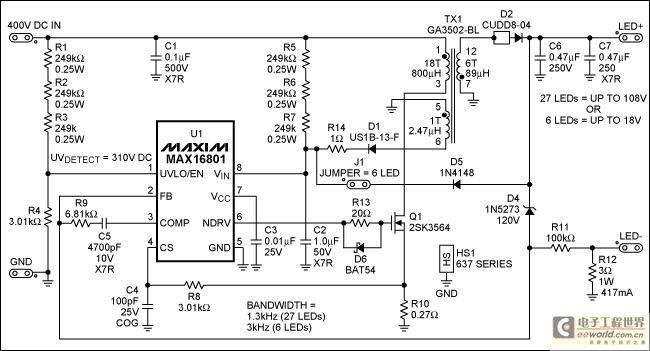
This reference design is a flyback LED driver for offline environments (400VDC). The design can drive 27 WLEDs (white LEDs) at 400mA. With the jumper, J1, installed, the design drives 6 amber LEDs at 400mA. The design uses the MAX16801 HB LED controller and a three-winding transformer (coupled inductor). There is no electrical isolation as the current sense is fed directly into the IC control loop.
The transformer has an 18:6:1 turns ratio. Primary inductance is 800µH with a current rating of 750mA (peak) and a duty cycle always less than 50%.
The frequency of operation is 265kHz and is nonadjustable. Overvoltage protection (nonlatching) is at 120V. The UV detect level is 310V. The turn-on delay time is about 43msec, after which VIN will be about 22V and the IC will begin to drive the external MOSFET. This will, in turn, cause the VIN capacitor to decay until the bootstrap winding can provide support. Because of the high impedance of the LEDs at low voltage, the main secondary load will initially be only the output capacitor. The secondary-to-tertiary turns ratio is 6:1, which means that the bootstrap winding will supply 10V to the IC as soon as 60V develops across the output capacitor. For the 6-LED string option (i.e., with J1 installed), the output capacitor must, obviously, charge to 10.7V before 10V is available to the IC.
The calculated peak current in the primary winding of the inductor is 750mA. Leakage inductance is minimized by a split primary that sandwiches the secondary winding. The primary leakage inductance is measured at less than 5µH. Because of this low value, there is no special provision for dissipating the leakage inductance energy; all leakage energy is dissipated in the MOSFET itself. The transformer temperature rise is less than 30°C.
The switching MOSFET has an isolated tab, which allows the heatsink to be connected to ground. This minimizes the metallic surface area that experiences high-speed voltage transients, and, in turn, minimizes radiated EMI. The MOSFET sees less than a 40°C rise in temperature.
| VIN: | 400VDC ±10% |
| PWM: | N/A |
| VLED config.: | 27 LEDs (2.8VDC to 4VDC) in series (75.6VDC min to 108VDC max); 400mA With jumper: 6 LEDs (2VDC to 3VDC) in series (12V min to 18V max); 400mA |

Figure 1. The LED driver reference design is 1.9in x 3.9in, double sided.

Figure 2. Schematic of the LED driver reference design.

More detailed image (PDF, 36.88kB)
Figure 3. Board layout of the LED driver.

More detailed image (PDF, 88.75kB)
Figure 4. Transformer specifications.

上一篇:利用超低电流、脉冲频率调制(PFM) DC-DC转换器降低
下一篇:MR-16 LED驱动器和用于脉冲LED冷却器供电的5V辅助
- 热门资源推荐
- 热门放大器推荐
- 打破台积电垄断!联电夺下高通先进封装订单
- Ampere 年度展望:2025年重塑IT格局的四大关键趋势
- 存储巨头铠侠正式挂牌上市:首日股价上涨超10%
- Vishay 推出新款精密薄膜MELF电阻,可减少系统元器件数量,节省空间,简化设计并降低成本
- 芯原推出新一代高性能Vitality架构GPU IP系列 支持DirectX 12和先进的计算能力
- NXP 2.5亿美元收购Aviva,但车载SerDes领域依然处于战国时期
- 应对 AI 时代的云工作负载,开发者正加速向 Arm 架构迁移
- 沉浸式体验漫威宇宙,英特尔锐炫显卡为《漫威争锋》提供Day 0支持
- 艾迈斯欧司朗与法雷奥携手革新车辆内饰,打造动态舱内环境
- 《嵌入式-STM32开发指南》第二部分 基础篇 - 第7章DMA(HAL库)

 Verilog HDL数字集成电路设计原理与应用
 CA139AF3


 京公网安备 11010802033920号